Characteristics and Application of Vacuum Pad
BACKWith the rapid development of semiconductors and the progress of hi-tech industry in modern times, the production of the product has now evolved, following increased demand for “sophistication” and “automation”. In this regard, the “Vacuum Pad” is a product suitable for the semiconductor and photoelectric industries. To cope with this trend, our R&D Team has developed a variety of materials through continuous innovation and research such as NBR, Silicone, FKM, conductive NBR, conductive silicone and PEEK; further, they have also improved the footprint, ESD and Y-Rate during production.
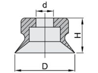 |
1-Step Model (Common): Typical Flat-type Pad, suitable for sucking the object on a flat and smooth surface to provide a stronger more stable suction force. |
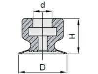 |
1-Step Model (thin type): Extremely thin lip of pad, suitable for working on a thin-type work piece. |
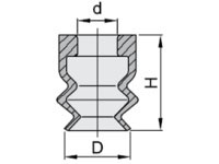 |
2-Step Model: Double-layer creases are configured on the pad, suitable for the suction of inclined object in providing a stronger and more stable suction force. By working with Engineering Plastics PEEK accessories, it can be used as a trace-free pad and anti-static ESD pad. |
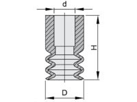 |
3-Step Model: 3-step design. Multi-layer creases are configured on the pad for shortening the travel effectively. When working on a work piece with bumpy surface, it allows the pad to achieve complete suction performance. |